This project is a complete implementation of the exercise 5.17 from Frank Vahid’s book “Digital Design” down to the electronic hardware level. This article will discuss general topics on the process design and all the code (in VHDL) will be available in a Github repository.
The example consists of an RTL project that provides a warning signal when the average of the four last temperature samples exceeds a user-defined value. The circuit has a 16-bit CT (current temperature) input indicating the current temperature, a 16-bit WT (warning temperature) input that indicates the warning temperature specified by the user, and a clear input button that disables the alert signal. When the Average temperature exceeds the setpoint specified by the user, the circuit activates output W (warning), enabling the alert signal. The alert output remains at a high logic level until the clear button is pressed.
The Projecting phase
In chapter five of Frank Vahid’s book “Digital Design”, the author enumerates the four phases of any RTL project. They are as follows:
- Get a high-level finite state machine that describes the expected final behavior.
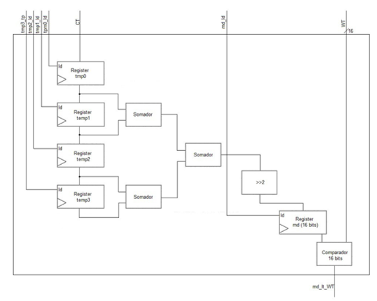
- Create an operational block that is capable of executing all the logic and arithmetic functions necessary for the expected final behavior.
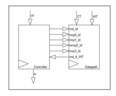
- Connect the operational block to a control block.
- Describe the expected behavior of the control block with a low-level finite state machine.
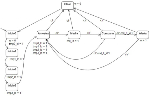
Down below are each and every one of the four diagrams representing every phase of the aforementioned process.
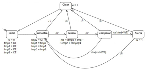
The high-level finite state machine
The coding phase
Once the projecting phase was done all the necessary information for executing the project was available. The project was implemented with an FPGA chip coded in VHDL. All the code is available in this link. The code used a structural style for streamlining the collaborative coding process and was test benched with ModelSim-Altera.
The Hardware phase
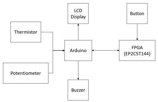
Once the code was ready and tested the next step was to upload it to the FPGA. The FPGA KIT EE02 (with an Altera EP2C5T144) was used. An Arduino Mega was used to read the analog signals and translate them to a 16-bit digital signal. An LCD display was added to the Arduino to view the variables in real-time. The clear Button was connected directly to the FPGA board, but the buzzer (warning signal) was connected to the Arduino because it worked with 5V and the FPGA’s logic levels were 3.3V.
In the video below it is possible to observe the final assembly working properly. During the video, the thermistor is brought close to the lamp and then far from it in order to cause a temperature variation.

